Translation of printed circuit boards using photoresist. Manufacturing a printed circuit board using a photoresist. The essence of the method and its difference from the LUT technology
Today I will tell you about the manufacture of a printed circuit board using film photoresist or the so-called photoresist manufacturing technology. printed circuit boards... Do not shout that LUT is cooler, cheaper and faster - I do not argue, but the photoresist has a higher resolution and is able to give results where LUT may not work. All of the following will apply to negative film resist. In my practice I use PF-VShch-50. The process of manufacturing a board using film photoresist can be divided into the following stages:1) preparation of the board blank and photomask;
2) applying a photoresist to the workpiece;
3) illumination of the workpiece with a photoresist through the template;
4) development of the board drawing;
5) etching the board.
We cut the workpiece out of foil-clad material with an allowance of at least 5 mm to the main size on each side. We print the template on film for the printer that is at hand. I have a laser and I print on universal double-sided film for laser printers and copiers. Whoever has an inkjet, then, accordingly, we take a film for inkjet. When printing in the laser settings, we select the maximum print quality, turn off the toner saving - the more there is on the template, the better. As a result, we have the following:
The printer is old and the cartridge has been refilled a bunch of times, so the print quality is poor. Therefore, the toner on the template is transparent enough, but we need it to transmit as little light as possible, i.e. it is necessary to increase the optical density of the image. For these purposes, there is a means for increasing the optical density of the negative Density Toner, but it was not possible to find it and it costs decently. I decided to use acetone - it turned out to be more than enough for my needs: we moisten a piece of medical cotton wool in acetone, throw it into a glass jar, put the template inside the jar with a pattern, twist the lid and set it to heat.

Heating can also be carried out on a radiator or even like a thread (depends on imagination). This process requires control so as not to overexpose the template in acetone vapor, otherwise the entire pattern will drain to the bottom of the can. In the photo, the template that has passed a pair of acetone - it has become somehow more black and shiny, try it - the result will be on your face.

We proceed to applying the photoresist to the workpiece foil, for this we stock up on approximately the following tools:

We roll out a roll of photoresist and cut a piece with a knife along the workpiece with a small margin on the sides, because it will not work perfectly evenly.

Now we take the "zero" and under a stream of cold water we begin to clean the foil of the board blank from the oxide film. A sign of the absence of an oxide film is a uniform coating of the foil with a water layer and the absence of drops.

Now we separate the bottom (matte) film from the cut out piece of photoresist. This can be done with the tip of a cutter or with a needle. Separate the film approximately 5-10 mm wide and glue the photoresist to the workpiece so that there are no air bubbles.

Now gradually pulling out the film, roll the photoresist onto the workpiece with a roller. After rolling, we cut off the protruding sides and roll the workpiece in the laminator.

Now we proceed to the illumination (exposure) of the billet. I use a COMTECH CE ST 26 E27 BLACK lamp as a radiation source. At this stage, it is necessary to choose the right exposure time (see comments to the article). We lay the workpiece on a hard, even surface, put a template on top and cover it all with ordinary window glass, and install a lamp on top.

We cover the workpiece with a book or other material that does not transmit light, turn on the lamp and let it warm up for a minute.

Remove the opaque coating and time it for normal exposure.

As soon as the time required for illumination has expired, turn off the lamp, remove the workpiece in a dark place and go to prepare the developer. As a developer I use soda ash (detergent), it is sold in household goods at a price of about 20 rubles per 0.5 kg. For cooking, take a teaspoon of baking soda and dilute with 1 glass of cold water.

Now we take out the illuminated workpiece, separate the upper glossy film, throw the workpiece into the developer and with three toothbrushes - a drawing of the future board begins to appear on the photoresist.

We continue to "clean" the future board until all the extra photoresist is washed off and we get this:

We wash our future board under cold water and throw it into the pickling solution to swim.

For etching, I use ferric chloride, and to speed up the process, I glue the board to a piece of foam with double-sided tape and lower it with the pattern down. In this case, it is necessary to check whether air bubbles remain under the board, otherwise they will not stain. After 10 minutes, we get the following result:

Now you need to wash off the remaining photoresist and here you can go in 3 ways:
1) throw the board into caustic soda (CAUTION! ALKALI! WORK IN GLOVES!);
2) boil the board in the solution in which it was developed;
3) throw the board into the solution in which the workpiece was developed.
The choice of method depends on the time it takes to make the payment. The longest is soaking in the solution in which it was developed (I throw it there overnight). Boiling in the developer takes about a couple of minutes. I don't know the time for caustic soda, but they say that it is also very fast.
It remains to bring our board to the required size, tk. we made allowances on each side and we can drill and solder our device. But to give the board beauty and improve solderability, it is still better to carry out tinning of the conductors. Someone with what, and I - with a fusion of Rose, as it turns out very quickly. For this I take the following ingredients:

Pour a glass of water into a bowl with a flat bottom and add a spoonful of citric acid (plays the role of a flux), throw the board there in the paths up and put a piece of Rose's alloy on top. We put all this on the stove and wait until the alloy begins to melt (it is better to hold the board with something).

The molten alloy is "rubbed over the board" (I use a brush with a piece of cotton wool wrapped around it). BE CAREFUL! STEAM CAN BURN YOUR HANDS! When rubbing, excess alloy is thrown into the water and only a thin shiny film remains on the conductors. We take out the board and rinse it with water. Now you can drill and solder.

Some comments on the technology:
1) The whole process takes approximately 1 hour.
2) When purchasing a photoresist, look at the date of manufacture. The shelf life is 9 months, after this period it does not stick well to the board. Store the purchased photoresist in a cold place (I have it in the refrigerator, it still sticks well, albeit expired).
3) You don't have a laminator to roll the photoresist to the workpiece? It doesn't matter - the iron will help. We turn on the thermostat to the 1st position and wait until the iron heats up. After heating to a certain temperature, the iron turns off, pull out the plug from the socket and put the board on the iron seam with the photoresist up, let the board warm up. We remove it and "from the heart" roll it with a roller.
4) When rolling the photoresist onto a wet workpiece and using a laminator, it is best to run the workpiece cold through the laminator to squeeze out the water. Otherwise, during hot lamination, water will evaporate and air bubbles will appear under the photoresist.
5) The choice of the exposure time of the workpiece through the template is as follows: A negative template with numbers from 1 to 10 is printed, applied to the board with the applied photoresist, and every minute the exposure is covered with an opaque material, one digit at a time, starting from 1. After development, you will see how many minutes light up. I have a 26W lamp, the distance from the workpiece to the lamp is 12 cm, the glass thickness is 4 mm - the exposure time is 3 minutes, I tried it for 5 minutes - it also works. I take a photoresist from the same manufacturer - the time is const.
6) Rosa can be tinned with an alloy in glycerin, but you can get it from your family for the "fog" arranged in the kitchen.
7) When soldering a tin-plated board with flux, it must be washed off immediately after soldering, otherwise the flux causes darkening of the Rose alloy.
8) Photoresist is not afraid of light from incandescent lamps, so you can work with light.
We take a textolite with dimensions larger than the future board by 10 millimeters and clean it. For these purposes I use a sponge for cleaning chrome.
The plus is that it removes the oxide layer while not picking up like sandpaper. Next, wipe it with alcohol, acetone, solvent or wash with soap, it's to your taste, as you like. Personally, I use a brake cleaning spray.


Knurling. Here I will dwell on in more detail. I do not know whether the photoresist is too good or too new, but if you apply it to copper, it will not work. Grabs to death. The first attempt was carried out like this. Tore off the protective film from the edge. This one is matte. Then he applied it with a corner to the copper and gradually, pressing it with his finger, pulled out the film. It stuck well, but there was dirt and bubbles ... In short, I switched to the principle of toners. We take a two-cube syringe and fill it with plain, cold tap water. Then we tear off the protective film completely. We hold the photoresist with one hand, with the other we pour water from the syringe onto the copper. The syringe is more convenient, since the copper is defatted and the drops roll down, and the syringe dispenses a little over the entire copper. After wetting, apply a photoresist. While the copper is wet, the photoresist freely crawls over it, and the water pushes out all the debris and air. And even if something went wrong, you can always tear it off the copper. After fitting from the center to the edges, using a rubber spatula, without pressing, we expel the water. When all the water comes out, we begin to squeeze out the remnants with force, also from the center to the edges. The photoresist will start to knock closer to the edges. It's OK. Pressing with a spatula from the center, it stretches quite easily and fits well.

After ironing, wipe it off with a napkin or toilet paper, it doesn't matter. The main thing is to wipe dry. We take a sheet of blank paper and fold it in half. Put textolite with photoresist between the halves and close this sandwich.

Well, here is someone like, someone with an iron, someone with a hairdryer, personally I am with a laminator. We heat the laminator at the highest temperature. After warming up, we send our sandwich there. Attention!!! If you send it to the laminator without a sheet of paper, then the pieces of photoresist, those that stick out outside the PCB, will be wrapped around the hot rollers and it will not be easy to tear it off from there.

I run it through the laminator twice in order to warm it up thoroughly. As a result, I get such a thing.


Sample. There are three options here. The first is typography. Well, given her absence next to my house, this option immediately disappeared. The second is printing on paper using a laser printer, then enlighten with a transparency. Well, I don’t have this muck. And the last one is printing on film. The laser has given poor quality, or rather not bad, but rather transparent toner. Keep over acetone vapor ... No ice for two reasons. The first is that it stinks, and they will kick me out of the house, and the second is that now for some reason acetone has been replaced with some nasty thing, which leaves drops of water after evaporation. Therefore, I switched to an inkjet. In addition, I have it sharpened for pictures. The film "Lomond" was chosen for printing.

She has one drawback. The surface on which you need to print is quite sticky and any debris sticks to it, and this, as practice has shown, negatively affects the quality of the board. In short, if the distance between the tracks is 0.2 - 0.1 mm, then a speck of dust can play a bad role and create a gap between the tracks. Otherwise, this film makes great templates.


Oh yeah, I almost forgot. The template needs to be printed on the collar for an eversion, that is, a negative. Where to etch the copper black, and where to leave it transparent. And don't forget to mirror. The important thing is that the paint should lie on the copper, and not vice versa with the paint up. In general, we put the template on a photoresist and all this under a UV lamp. I have so:

Here we will dwell in more detail. Lamp: Model ELSM51B-Color 20W Black. As you can see in the photo, energy saving. Purchased from "Chip-dip" for 200r. The distance from the lamp to the PCB is 20 cm. Taking into account the fact that the glass retains UV light, it is impossible to specifically stipulate the exposure time, since someone will tear off 6 mm glass from the sideboard, someone 3 mm from the entrance window. I bought in "OBI" a photo-frame made of dense wood in the size of 300 x 200. The pieces of iron and cardboard went straight to the trash heap, and the glass 2 mm thick went to the clamp. I used the frame itself to stretch the mesh for applying a solder mask. But this is a topic for another article. So I have 2 mm glass. I use two 7 Ah gel batteries for the load. In this form, the illumination is seen exactly two minutes from turning on the lamp to turning it off. I do not warm up the lamp, since 20 watts is quite powerful. As a result, I get an overexposed photoresist. Another plus against ours, after development, the exposed areas darken and you can see what happens. Next, we prepare the bath. On a glass COLD !!! water half a teaspoon of soda ash. The water should be at room temperature. If you take a hot one, it will be like with our photoresist. All the tracks will fall off. After preparing the bath, we bathe the textolite.


If you help with a brush, the development will take less than a minute. As a result, we will get this kind of beauty.


We dry, we look. If something is wrong somewhere, we will correct it. If you can't fix it, then we start all over again. Another plus against our photoresist. After exposure, we throw it into the soda ash solution for 30 minutes and the photoresist will fall off by itself. I could not tear off the domestic one, neither with acetone, nor with soda. In short, I threw out the spoiled workpieces. After all the checks, we poison in a pickling solution. Here it is every man for himself. Some in acid, some in vinegar, I personally prefer ferric chloride. Preferably water, otherwise waterless, if you throw it into the water, there will be an explosion :)

Well, after etching, as always, drilling and applying a solder mask, but this is the topic of the next article.


That's like with a photoresist and that's it, if you have any questions, write either in the comments or on the forum.
All good boards.
Andrey 04/05/13
Great article. I did everything as written, it worked the first time. Now someone else would write the same article about metallization :)
SergeBS 04.21.13
Some kind of game. 1. "In short, if the distance between the tracks is 0.2 - 0.1 mm, then a speck of dust can play a bad role and create a jumper between the tracks.". The photoresist is negative (see below for the template). A speck of dust will not let the track light up and, as a result, a track break, not a short circuit. 2. "I use two 7 Ah helium accumulators for the cargo." There is no HELIUM in the batteries, but there is GEL. And it is not at all necessary that there is gel in maintenance-free batteries. Gel batteries are rare. 3. "As a result, I get an overexposed photoresist. Another plus against our
SergeBS 04.21.13
Truncated comment. OK. Let's repeat. Some kind of game. 3. "As a result, I get an overexposed photoresist. Another plus against ours, after development, the overexposed areas darken and you can look at what will turn out. Next, we prepare a bath. In a glass of COLD !!! water, half a teaspoon of soda ash. The water should be at room temperature. . If you take a hot one, it will be like with our photoresist. All the tracks will fall off. After preparing the bath, we bathe the textolite. If you help with a brush, the development will take no more than a minute. As a result, we are half
SergeBS 04.21.13
As a result, we will get this kind of beauty. "We will not get NIFIGA. Before etching, you need to peel off the protective Mylar film from the surface of the photoresist. Regardless of the origin of the film photoresist. (Import or Russia). So this is:" Andrey 05.04.13 Excellent article. I did everything as written, it turned out the first time. "Lies. Miracles do not happen, it does not etch through the film. And if you tear off the film before exposure, the photoresist will stick to the glass. 4." Dry, look. If something is wrong somewhere, we will correct it. If you can't fix it, then we start all over again.
SergeBS 04.21.13
Wonderful:). The photoresist flew off - pure copper remained - it's time to etch. Even if we assume a miracle that something (even soda, even ferric chloride) crawled through the unremoved protective film ... so that the photoresist flew off. About the explosion, a joke of humor, well, is completely out of place, too. Someone, after all, can believe. So you need to edit this magnum opus. And in the future, do not fill a review for yourself (this is about the mythical Andrey, who did as in the article and he succeeded :)). Read comments from bottom to top, "stitching" over identical pieces of text.
SergeBS 04.21.13
Total. CORRECT: 1. Negative template. You can use the laser. I have no inkjet - but everything is fine. 2. Peel off the bottom matte plastic wrap. 3. Glue it and let it lie under the load. 4. Highlighting - the template with paint (toner) to the photoresist.
SergeBS 04.21.13
5. After exposure - a pause of 30 minutes. Then we tear off the top shiny protective lavsan film and develop in baking soda. In a weak solution (citric acid - a teaspoon per glass) we tan the manifested. 6. In warm water we throw a little (so as not to boil) ferric chloride and we poison in it.
SergeBS 04.21.13
7. Etched - in any alkali ("Mole" diluted 1:10 - 1:50 is that). In 10-15 minutes, the photoresist will fly off. 8. We wash with water (it is possible with liquid detergents). 9. We drill, tinker, solder the parts. Everything. In short, we do it according to the instructions ...
Alexey 04/21/13
Dear SergeBS 1 about the film. Describe its removal? You may be offered to learn Russian, otherwise how will you read an article, it is written in Russian. 2 With the battery, this is just a banter for the sake of scribbling. What's the difference than pressing. For example, I have replaced them now with two trances. And that there are few photos in the article. By the way, this board works and feels great. And in the end there is a section "Write an article", you write, and you will be criticized, then we'll see. And everyone can shout and throw mud.
Alexey 04/21/13
Oh yes, at the expense of the laser. Neither XP nor Xerox provide quality templates. I've tried everything. Especially if with a domestic resist, then it is stupidly illuminated as if there is no template at all. Maybe, of course, they sold me an old resist ... And even if, according to your scheme, to tear off protective film and try to glue it, and then under the load.)))) Well, well.
Vitaly 05/14/13
Alexey, a very wonderful article. I have a great desire to do all this, to begin with, buy everything you need (if you can help with this, I will be very grateful). And what kind of inkjet printer did you use.
Alexey 05/14/13
At first I had an Epson Stylus CX4300 but the head on it dried up. I have now bought an Epson L110. It is designed for continuous use and the ink is poured from the side into flasks, not cartridges. According to my measurements, black paint is enough for 50 sheets of A4 solid fill. And of course, ink is much cheaper. If you have any questions, please write. I will definitely answer.
Mikhail 05/16/13
Hello. The article is actually good, this is me, as a person who has been making boards for more than 15 years. SergeBS, why are you broke? Write your article, business. : +) And I have one question for the author: could you tell me what settings you set on the Epson L110 to print a template? Sincerely, Mikhail.
Alexey 05/16/13
Hello Mikhail. In the printer properties, select the "Advanced Settings" tab. In the "Color Correction" section, check the "Settings" box. The "Advanced ..." button will appear by clicking on which the settings menu will appear. In this menu, the brightness is at a minimum, and the contrast and saturation are at the maximum. Yellow at maximum (yellow delays UV) and magenta with cyan at minimum. And here's another, uncheck "High speed printing". Look like that's it.
Mikhail 05/16/13
What material / quality do you choose? In general, it's interesting, it's simple, I now also use the L100, and on the contrary, I removed the yellow one, otherwise it refuses to dry on the template (the film is the same).
Alexey 05/16/13
And there the quality is either automatic or manual. My material is just paper. Do they dry for a long time? What ink? Relatives, "Fool" or not original? It is important.
Mikhail 05/16/13
I have a lot of everything in the drop-down list. Normal, high, photo, best photo ... I am currently printing using Photo RPM (max dpi) with saturation up. Prints slowly, a bunch of passes, but the quality is perfect. Only here it is the yellow color that dries for a very long time. And the ink is native, which came in the kit.
Alexey 05/17/13
Well, in principle, this is the very thing. I set it up on the old one. How long do they dry? If about 10 minutes, then you can roll the photoresist at this time. :)
Alexey 11/22/13
For some reason, in the space between the 0.1 0.2 mm tracks, the photoresist in soda does not come off well .. you have to hold and help with a brush longer and at the moment when this space is cleared, in other places with thicker tracks the pads are already pads and the tracks themselves fly off ..
Alexey 11/23/13
Try to reduce the exposure time by 10-15 seconds.
Alexey (friend 02/17/14
Hello Alexey! Thank you for the article. It's funny, but now I'm making exactly the same board for exactly the same controller, but not 100 but 103 series. I am suffering with PF-VShch. And my problems are exactly the same as you described. I have already taken out a sheet of 30x50 (my board is 5x6cm, i.e. about 50 samples), and the result is zero. I don’t give up yet. There is no other FR in our city. :(
Alexey 02/17/14
MarioFly 09/08/14
"Another plus against ours, after development, the exposed areas darken and you can see what happens." Not after development, but after exposure.
Anton 11/04/14
Yes, thanks, I also suffered with this PF-VShch. I thought that everything, my hands have grown to another place. And yet I took Ordyl for a try, so everything worked out right away. Even with a pattern with gaps (LED printer), it came out normally at minimal illumination.
Alexey 11/04/14
I give this PF-VSH in good hands))) a roll of 5 meters. True, the expiration date has already expired, but I think it's nothing ... My protective mask has expired as 2 years and nothing. So if there are those who want to try their luck with PF-VShch, write. And then it's like a suitcase without a handle, you don't need nafik yourself, but it's a pity to throw it away.
What we need:
- Film photoresist negative (for example, in AliExpress)
- PC and (optional SL5-SL6)
- Transparencies for inkjet or laser printers (such as this)
- Printer (for the corresponding film - who has which)
- Foil fiberglass
- Paper (plain) and eraser
- Sharp object (needle, scalpel, etc.)
- UV lamp
- Soda ash (baking soda will not work)
- Smooth hands
So, a negative film photoresist is a photosensitive polymer material coated on both sides with a thin protective film (such a sandwich in Fig. 1). Exposure to light either destroys the polymer (positive photoresist), or, conversely, causes it to polymerize and reduces its solubility in a special solvent (negative photoresist). During subsequent processing, etching occurs in the "windows" formed by overexposed (positive photoresist) or non-overexposed (negative photoresist) sections of the polymer.
For example, there is a ready-made layout of a certain device (let it be):

To make a printed circuit board, you must first make a photoresist photomask. For this:
- we climb into the menu "File" -> "Print"
- disable printing unnecessary layers
- scale 1: 1
- and put the checkbox "Negative"(if you forgot to put it and put it in print on the printer, you will have to reprint it) !!!
- you need to throw more paint onto the transparent film. Therefore, we climb into the printer settings and set:
- print quality: very high
- print type: black and white
- if there are other settings - see for yourself
Check points 2-4 again and send the template for printing (see the pictures below).
After - we check our template for transparency - the drawing should be clear and not show through (if you can see everything through it - it's a bad thing - you can print it again or print a new one (by changing the printer's print settings))


Here's the result:

In the meantime, our template dries up (do not leave your prints on it), we will prepare the basis for applying the photoresist - PCB foil. To do this, the copper coating of the PCB must be cleaned and degreased: we take the required size PCB and wipe the copper layer with an eraser in order to remove dirt from the copper. That's it, DO NOT touch this part of the PCB with your fingers! So that there are no gum particles left on the foil and again not to cover it with greasy hands, the copper should be slightly polished to a shine with paper (but NOT PRESENT!).

Next, we take our photoresist (the one that is the roll). Cut off the desired piece and hide the roll far away from the light (otherwise, over time, it may light up and the whole roll will disappear). You need to slightly pick up the matte protective film (it is located on the inside of the roll, see the figure) using a needle, for example.

Do not touch the part of the photoresist with which you are peeling off the film with your fingers, otherwise it will not stick to the copper.
Now, with a slight movement of your hand, we apply the photoresist to the board, press and gradually remove the matte film (photo). We carefully smooth out the whole thing (the photoresist should adhere all and so that without bubbles, etc., after smoothing, the board can be put between the pages of the book and pressed firmly)

While we were molding the photoresist to copper, our photomask managed to dry (hopefully). Now we apply it to the board with the photoresist (the side where it is printed, to the photoresist - if you did not print a mirror template). We align the template along the edges of the board and put glass on it (the template must be tightly pressed against the board, otherwise something that should not be illuminated may light up)
Now we put an ultraviolet lamp at a level of 10-15 cm above the board and light up our photoresist for about 7 minutes.
We remove the photomask and peel off the transparent film from the board (photoresist). This operation must be carried out carefully so as not to tear off the photoresist itself from the board.

Now we need to develop our photoresist. To do this, we soak our board in a solution of soda ash for 30 seconds. With light movements of the toothbrush on the surface of the board, we wash off the remnants of the unlit photoresist (while dipping the board in a soda solution). When copper is clearly visible, rinse the board with plain water and let it dry.

What problems can arise?
If the photoresist remains, where it should not be, then:
- Or overexposed with ultraviolet light,
- Or they made a bad photomask and through it the ultraviolet light illuminated everything
- The photomask was badly pressed against the photoresist (in this case, the tracks may be wider than necessary)
If the tracks themselves are torn off during the development of the photoresist, then:
- The photoresist does not adhere well to the copper -> the copper is poorly prepared (oily, dirty, etc. or the photoresist is broken (I did not have this, but anything can be))
- Necessary EASIER rub with a toothbrush
- Overexposed the board in water (solution) - after all, the photoresist was not glued to copper with superglue.
Well, if the photoresist is completely washed off during development, it means that the UV lamp was not illuminated enough.
And then everything is as in the scenario: ferric chloride ... etch ... wash off the remaining iron ... the photoresist can be removed with a knife, or with a solvent (which is much easier), or you can leave it as a protective coating for the tracks (so to speak).
The first time it may come out crooked, but with practice, mastery comes. Good luck!
Published 03/23/2012
In this article, I will show you how you can make PCBs at home with minimal discomfort for your home and minimal costs.
Laser-ironing technology will not be considered due to the complexity of achieving the required quality. I have nothing against LUT, but it no longer suits me in terms of the quality and repeatability of the result. For comparison, the photo below shows the result obtained with LUT (left) and with a film photoresist (right). The thickness of the tracks is 0.5 mm.

When using LUT, the edge of the track is torn, and there may be shells on the surface. This is due to the porous structure of the toner, as a result of which the etching solution still penetrates to the areas covered by the toner. This does not suit me, so I switched to photoresistive technology.
In this article, whenever possible, tools, utensils and reagents that can be found at home or bought at a household chemicals store will be used.
Photoresistive PCB Manufacturing Technology
A photosensitive layer is applied to the copper layer. Then, through a photomask, certain areas are illuminated (usually with ultraviolet light), after which unnecessary areas of the photosensitive layer are washed off in a special solution. Thus, the required pattern is formed on the copper layer. This is followed by the usual etching. You can apply photoresist to textolite in different ways.
The most popular methods are using an aerosol photoresist. POSITIV 20... This method is similar to the application of spray paints. Needs care to ensure an even layer and drying.
And the application of film photoresist. Apply by gluing a special film similar to how decorative films are glued. Dry film photoresist provides constant photosensitive layer thickness, easy to apply. In addition, it is indicative, i.e. overexposed areas are clearly visible.
What is Film Photoresist?

Please do not be confused with aerosol photoresist. Film photoresist consists of three layers of film. In the middle there is a photosensitive film covered on both sides with protective films. On the side that is glued to the PCB - soft, on the other - hard. Film photoresist has a number of advantages over aerosol. Firstly, it does not stink when applied, does not require drying. Very handy when working with a small number of boards. Unlike aerosol photoresist, where the thickness of the layer is difficult to guess, the thickness of the film photoresist is always the same. This simplifies the timing of exposure. Indicator film photoresist. Those. overexposed areas are visually visible.
PCB selection
If you want to get a high-quality printed circuit board with conductors less than 0.4 mm and a distance between conductors of 0.2 mm, you will need a normal textolite. The photo below shows two pieces of PCB. It is clear that the photoresist film will not fit well on a scratched, dirty textolite. Take the normal one right away. And keep it at least in a newspaper so as not to scratch it. The “left” textolite can be used if there are thick tracks (0.5 ... 1 mm) on the board and at least 0.4 mm between the conductors, and you do not have to show the board to strangers.

Preparation and cleaning of PCB
We cut the textolite into blanks of the required size. At home, this can be done with a hacksaw for metal. Textolite up to 1mm thick can be cut with ordinary office scissors. Remove burrs with a file or sandpaper. At the same time, we do not scratch the surface of the PCB! If the surface of the copper foil is dirty, or at least smeared with your fingers - the photoresist may not stick - goodbye quality. Since after “cutting” we have “dirty” textolite, chemical cleaning should be carried out.


We will carry out chemical cleaning of the copper coating before applying the photoresist using household chemicals. We clean the surface of the PCB with a descaling agent " Cillit“. It contains orthophosphoric acid, which removes all impurities. Therefore, we cannot put our fingers into this liquid. If there is no suitable container, you can put the textolite on the bottom of the bathroom and just pour it over with this liquid. After 2 minutes (do not overexpose), rinse thoroughly with running water. There should be no stains on the surface. Otherwise, repeat the operation. Remove the remaining water with a paper towel. We try not to bring the napkin to a state where paper pile will crawl out of it. It is because of the nap that I do not use cloth napkins. If even the smallest threads remain on the copper surface, the photoresist film will lie with a bubble in this place. Dry the textolite with an iron through paper. Do not touch the PCB surface with your fingers!

In some sources, you can find a recommendation to degrease the surface with alcohol. Personally, when cleaning with alcohol, the result was much worse. The photoresist did not adhere normally everywhere. After " Cillit”The result is always much better.
Photoresist sticker
Sticking photoresist film is the most critical operation in the production of boards using this method. The quality of the result obtained depends on the accuracy of this operation. All photoresist operations can be performed under low electric light. After drying, the textolite should cool down. The photoresist can also be glued to warm PCB, but you will only have one try. The photoresist film adheres tightly to a warm surface.
We cut off a piece of photoresist with a small margin, so that it completely covers our workpiece + 5 mm on each side. Using a sharp knife, gently pry off the soft film with a sharp knife (if the photoresist is in a roll, this is usually the inner side). Do not remove the top protective film yet!
We do not separate the entire protective film, but a small area: 10-20 mm from one edge. We glue on the textolite, smoothing with a soft cloth. Next, we slowly continue to separate the protective film and smooth the photoresist to the PCB. At the same time, we make sure that there are no bubbles, and do not touch the not yet pasted textolite with our fingers! Then we cut off the photoresist protruding from the edges of the workpiece with scissors. After that, you can slightly warm up the workpiece with an iron. But not necessarily. If you touched the workpiece with your fingers or there was a lint from the fabric or other debris on it, this will be visible under the film. This will negatively affect the quality. Remember, the quality of the result obtained largely depends on the thoroughness of this operation. The textolite prepared in this way is best stored in a dark place. Although electric light has very little effect on the film, I prefer not to risk it.
Preparing a photomask
We print the photomask on a film for a laser printer or on a film for an inkjet printer. Photo for comparison:

The template on the film for an inkjet printer is denser, a laser printer is worse in this regard - gaps are visible in dark areas. In case of exposure, you will need to pay attention to what type of photomask will be used and make an adjustment to the exposure time. It is not a problem to find a film for a laser printer, the price is more than affordable. You have to look for an inkjet printer, and it costs about 5 times more. But for small-scale production, the use of a photomask printed on inkjet printer completely justifies itself. The photomask must be negative, i.e. the places where copper should remain must be transparent. The photomask must be printed in mirror image. This is done so that when applying it to the textolite with photoresist, the paint on the film of the photomask adjoins the photoresist. This will provide a clearer drawing.
Projection
Since the article focuses on the use of household devices, we will use available tools, namely: an ordinary table lamp. We screw into it an ordinary ultraviolet lamp purchased from an electrical store. We use a CD box as a rack if there is no suitable plexiglass sheet.


We put our blank, a photomask on top and press it with plexiglass (cover from the CD box). You can, of course, use ordinary glass as well. From the school course, we remember that ordinary glass does not transmit ultraviolet rays well, so it will take longer to light up. Under normal glass, I had to double the exposure. The distance from the lamp to the workpiece can be selected experimentally. In this case, about 7-10 cm. Of course, if the board is large, you will have to use a battery of lamps or increase the distance from the lamp to the workpiece and increase the exposure time. The exposure time for the photoresist is 60 ... 90 seconds. When using a photomask printed on a laser printer, the shutter speed should be reduced to 60 seconds. Otherwise, due to the low density of the toner on the photomask, the covered areas may light up. Which will lead to difficulties in the development of the photoresist.

A very important operation is the heating of the workpiece after exposure. We put the iron on “2” and heat it through a sheet of paper for 5-10 seconds. After which the drawing becomes more contrasting. After warming up, let the workpiece cool down to at least 30 degrees, after which you can start developing the photoresist.
Photoresist development
There are special developers for the photoresist that can be purchased at specialized electronics stores. On the Internet, you can read what you can show with soda, but always caustic (caustic soda is caustic sodium (NaOH)). I bought a special developer, which is nothing more than this caustic sodium (NaOH). Then, in order not to throw money down the drain, I bought a tool for cleaning pipes "Mole", in fact, it contains the same caustic sodium (NaOH), but nothing else is included in it.
But I refused them, because I have to work with gloves (the solution is dangerous and corrodes the skin). The process is very fast. In addition, it is completely unacceptable to keep such a solution in a house where there is a wife and small children who can find this dangerous liquid.
Therefore, we take simple baking soda. Baking soda is not only a safe chemical that is easy to buy at the grocery store, but it is also much more enjoyable to work with. It does not dissolve the photoresist film so quickly, so it is difficult to overexpose the photoresist in the solution. Washing out unlit areas of the photoresist is more delicate and less rapid. The fact is that the removal of the photoresist film from the finished board is performed in the same solution, so if you overexpose, the photoresist will start to lag behind the PCB.
We prepare the solution according to the following recipe: pour baking soda into a bottle, no matter how much it is, pour hot water, dissolve by applying reciprocating movements to the bottle, i.e. pounding. Attention! If you are using sodium hydroxide (NaOH), the concentration should not be so severe. A teaspoon per liter is enough.


Next, pour the solution into a cuvette or shallow container. We separate the upper protective film from the photoresist film (it is more rigid than the first one, it can be separated by hand), immerse the workpiece in the solution. After 3 minutes, take it out and wipe it under running warm water with a soft sponge for washing dishes. Then back into solution for 2-3 minutes. And so on until the photoresist is completely washed off from the underexposed areas. Then we rinse the workpiece well in running water.
Etching
Solution: The most popular etching solution for printed circuit boards is ferric chloride. But I got tired of the red spots, and I switched to ammonium persulfate and then sodium persulfate. Details about these substances can be found in search engines. On my own behalf, I will say that the etching process is more pleasant. And although sodium persulfate is somewhat more expensive than ferric chloride, I still won't give it up, because it's good.
Dishes: The ideal pickling dish is a special heated container with a circulating solution. You can make such a device yourself. Heating can be done from running hot water or electric. Aquarium technologies can be used to organize the circulation of the solution. But this topic is beyond the scope of this article. We will have to use household products. Therefore, we take a suitable container. In my case, it is a transparent nylon vessel with a tight-fitting lid. Although not required, the lid simplifies the pickling process, and the solution can be stored directly in the pickling container.
Process: We know from experience that the etching process is faster if the solution is heated and stirred. In our case, we put our container in a bath under a stream of hot water and periodically shake it to mix the solution. Sodium persulfate solution is transparent, so there is no difficulty in visually monitoring the process. If the solution is not stirred, the etching may not be uniform. If the solution is not heated, the etching process will take a long time.

Upon completion, we rinse the board in running water. After etching, we drill the board, cut it to size.
Photoresist cleaning, preparation for tinning

It is better to wash the photoresist after drilling. The photoresist film will protect the copper from accidental machining damage. We immerse the board in a solution of the same baking soda, but heat it up to speed up the process. The photoresist lags behind in 10-20 minutes. If you use caustic sodium (NaOH), everything will happen in a few minutes, even in a cold solution. After that, we thoroughly rinse the board with running water and wipe it with alcohol. It is imperative to wipe it with alcohol, since an invisible layer remains on the copper surface, which will interfere with the tinning of the board.
Tinning
How to tinker? There are many ways of tinning. We assume that you do not have special devices and alloys, so the easiest way will suit us. We cover the board with flux and tinker with ordinary solder using a soldering iron and copper braid. Someone is tying the braid to the soldering iron, I have adapted to hold the soldering iron in one hand, the braid in the other. In this case, it is more convenient to use the PCB holder! For tinning boards I use this one (it is easier to wash). But you can also use an alcoholic solution of rosin.


P.S.
Finally, a list of materials and tools that we needed:
Materials (edit)
- Photoresist film
- Foil-laminated textolite
- Means " Cillit»
- Paper napkins
- Baking soda
- Alcohol
- Ferric chloride or ammonium persulfate or sodium persulfate
- Solder
Instruments
- Scissors
- Sharp knife
- Flat file or sandpaper
- Dremel or drilling machine, which is able to hold drills from 0.8 mm., Drills
- Dishes for developing photoresist
- Pickling utensils
- Small piece of soft cloth
- Iron and blank paper
- UV lamp
- Table lamp
- CD box or a piece of plexiglass
- Inkjet or laser printer and film therefor
- Soldering iron
- Copper braid (can be purchased, can be removed from coaxial cable)
- Foam sponge.
To illuminate the photoresist at home, I decided to use an A4 scanner, which I have successfully "died", and you can buy a big one for this purpose, for example, starting from 100 rubles (a pack of cigarettes is more expensive, and a faulty one is can give).
In general, I decided to breathe a "second life" into the scanner, especially since there is quartz glass, which transmits ultraviolet light very well (a simple window glass, as we know, is a maximum of 10%). Another advantage of this method is the uniform pressing of the board against the glass by the scanner lid and a constant distance to the UV source, due to which the exposure time becomes constant, which can be fixed with a simple timer.
In the end, this is what happened:
Picture 1.
PP illuminator with photoresist.
Disassembled the scanner, threw out the insides and replaced them with four lamps. For this purpose, I used accessories from ordinary fluorescent lamps, only I installed UV lamps (all this is sold in household goods stores). Maybe two lamps would be enough, the boards are still not very large in general, but, as they say, the stock does not pull, so I decided what to do, so to do this with a view to the future (for an A4 board), so I installed four, and the exposure time in this case will be shorter.
To control the illumination process, I use a countdown timer, which was collected on the PIC16F628 microcontroller. As a result, the whole process of illumination of this structure takes 30-40 seconds ...

Figure 2.
Device design.
Someone might say that it would be possible to assemble a timer inside the scanner and not bother with the case. I do not argue that this option is quite suitable for someone, but suddenly I need a timer separately, for some other purpose, so I decided to make it in my own case and in the form of a separate finished structure.

Figure 3.
Timer circuit.
On the Internet, if you dig a little, there are many different schemes of all kinds of timers. I settled on this scheme, I just had a PIC16F628 in stock, and I decided to put it into action.
Maybe you will like another timer scheme - this is your choice, I just tell the process itself, well, I give a description of my designs.

Figure 4.
Timer circuit, power section.

Figure 5.
Timer in the case.

Figure 6.
Power section.
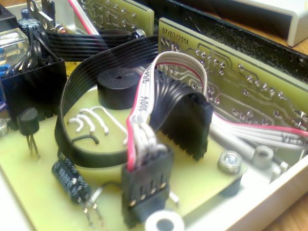
Figure 7.
Boards and connections.
The maximum time that can be set on the timer is 12 h 00 m 00 s. After setting the time and pressing the "Start / Stop" button, the load is switched on and the time countdown begins in the reverse order from the set one. 10 seconds before the end of the time - a short sound signal is sent to the "buzzer".
When there are 3 seconds left before the end of the time, the "buzzer" turns on until the end of the time. At the end of the time, the load is turned off, the time on the timer is set to the one that was set at the beginning with the buttons.
Now I will briefly describe the process of manufacturing printed circuit boards using a photoresist. Everything described above was intended to simplify this process.
For work I use a film negative photoresist. Negative, which means that the template for its exposure must be printed in negative, that is, the places where the tracks will be should be transparent, and where there should not be tracks (foil), toner is applied. If you use a positive photoresist, then naturally the photomask will need to be printed in positive.
We print the template through the program for designing boards in negative on transparent film (I use LOMOND film for inkjet printers) on an inkjet printer. I tried it on a laser, but it turned out somehow faded, there was no blackness, and the boards were not quite high-quality.
They say that you can greatly improve the quality of such boards if you print two templates on a film on a laser printer, then cut them out and combine them (that is, make one out of two).
You can also print a drawing of the board laser printer on plain paper. The thinner the paper, the better. Further, to increase the contrast (if it is not sufficient), immerse it in a can of solvent (for example, an automobile 647) for a split second. Let it dry, and then soak it with sunflower oil to make it transparent to ultraviolet radiation, though I have not tried that.
We are preparing the blank of our future board in size a little larger than required. Then the foil must be prepared for gluing the photoresist.
There is no point in repeating how all this is done, since this process is described on dozens of sites. Just type in the search engine "manufacturing of PP using a photoresist", and you will have a bunch of options, after reading a couple of them, you will have an option that is right for you.
We will assume that the board has already been prepared and the photoresist is glued (or applied from a spray can) to our board.
We apply the template to the board. As a rule, the template fits tightly to the board. And put it on the scanner glass with UV lamps. Highlighting. We remove the exposed workpiece in a dark place and prepare a solution for development, for which I use soda ash (sold in household stores it is used to soften water and costs a penny).
To do this, dissolve a teaspoon of soda with a slide in a liter of water (if the board is large), or a flat spoon in 0.5 liter of water.
We take our board from a dark place, remove the top protective film from the photoresist and put it in our solution with diluted soda and wait about 30 seconds. Then we take a brush and start driving it around our board in order to speed up the process of washing off the photoresist from unnecessary plots. Where the photoresist has washed off, the copper surface is light and shiny. After all the unnecessary photoresist has been washed off, we take the board out of the soda solution and rinse it under running water.

Figure 8.
A printed circuit board prepared for etching.
After washing, dry the board. We examine. It may happen that there are stains (where the photoresist was not well glued). We use a marker to draw printed circuit boards. We retouch where necessary. Photo # 8 shows that where the photoresist is not of high quality (my expiration date has already expired) those places are retouched with a black marker.
The attachment below contains files for making a timer. Source, firmware, pp.
Archive for the article.


